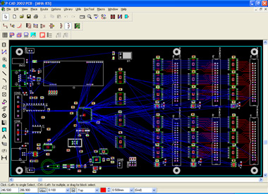

PCB Design

In addition to laying out PCBs for products we are designing in house, we offer PCB design services independently to customers seeking this service. Our portfolio includes "in-house" and "on-site" services. All of our designers are fully accredited in the use of PCB software and design tools. Most have at least 10 years experience in PCB layout.
Design tools used include ALTIUM, MENTOR (GRAPHICS), CADENCE, ALLEGRO, CADSTAR, ACCEL, PADS and various legacy tools.
We offer our considerable experience in most design disciplines, which include:
![]() digital
digital
![]() analogue
analogue
![]() high-speed designs
high-speed designs
![]() RF
RF
![]() microwave
microwave
![]() impedance routing
impedance routing
Advanced technologies :
![]() Rigid, flexible and flexi-rigid PCBs
Rigid, flexible and flexi-rigid PCBs
![]() Sequential laser drilled, micro-via PCBs and buried/blind vias
Sequential laser drilled, micro-via PCBs and buried/blind vias
![]() Buried components (resistors and capacitor).
Buried components (resistors and capacitor).
![]() Copper-invar-copper and exotic substrates.
Copper-invar-copper and exotic substrates.
We design for conventional component packaging, and also:
![]() SMD (BEA, MCH-L), TAB, and buried components.
SMD (BEA, MCH-L), TAB, and buried components.
We operate a fully flexible approach. Designers can be supplied to work as a contractor on your site, or we can operate as a sub-contract service from our offices - or as a permutation of these, if you prefer.